The journey of IoT module design has been marked by continuous innovation in the pursuit of smaller, yet more efficient form factors. The introduction of the Land Grid Array, or LGA, has marked a significant advancement in the cellular IoT domain. LGA-based modules offer exceptional performance, ease of integration, and cost efficiency in IoT applications. The latest statistics show that the demand for LGA packages is rising globally.
The LGA Packaging Market size, estimated at USD 386M in 2023, is expected to reach USD 727.75M by 2032, exhibiting a CAGR of 7.30% during the forecast period.
-Global Land Grid Array (LGA) Report 2025-2032, Semiconductor Insight
Evolution from Pin Grid Array to Ball Grid Array
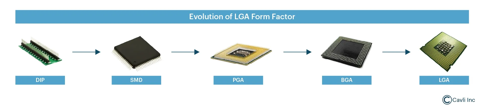
Dual In-line Package- The Pin-Based Packaging
The Dual In-line Package (DIP) is one of the earliest packaging technologies used in embedded systems. DIP components have two parallel rows of through-hole pins inserted into a Printed Circuit Board (PCB).
DIP’s advantage is its ease of prototyping, which is ideal for early hardware design and testing. It provides an easy way to repair and replace components manually without specialized equipment. It is suitable for small-scale production with lower initial manufacturing costs.
Surface-Mounted Device (SMD)- The Compact and Automated Packaging
While large space consumption, limited pin count, and mechanical fragility made DPI unsuitable for IoT devices, the Surface-Mount Device (SMD) modules marked a significant shift in electronics manufacturing.
SMD modules use small solder pads mounted directly onto the PCB using Surface-Mount Technology (SMT). The advantages of SMD Modules are minimal PCB space usage, automated assembly with SMT techniques, and improved electrical performance with reduced signal loss. Soon, SMD became the preferred choice for IoT modules due to its space efficiency. However, pin-based connections were still a limitation, leading to the development of pin-less alternatives like LGA.
Pin Grid Array (PGA) – A Denser Pin-Based Alternative
A Pin Grid Array consists of a grid of pins on the underside of the chip that fit into corresponding holes on a PCB or a socket. PGA was used for microprocessors and embedded systems. For example, AMD utilizes the Pin Grid Array (PGA) form factor in its Ryzen and EPYC processor series.
PGA packages can be either:
Socketed PGA (SPGA) – Inserted into a socket on the PCB without soldering.
Soldered PGA – Directly soldered onto the board, making it permanent.
While PGA packaging had benefits in computing and embedded systems, it did not get widely adopted for cellular IoT modules due to:
- Large footprints: PGA is too large for miniaturized IoT applications.
- Fragile: Bending or breaking of pins could cause device failures, making it unreliable for industrial and outdoor IoT.
- SMT techniques: PGA lacks automated SMT production and high-reliability soldering.
- Thermal efficiency: PGA fails to provide optimized thermal dissipation in cellular IoT modules.
Ball Grid Array (BGA) – The First True Pin-less Alternative
Ball Grid Array (BGA) was introduced to overcome the pin fragility of PGA and the limited connection density of SMD. Instead of pins, the Ball Grid Array uses solder balls arranged in a grid pattern on the underside of the package. This pattern allows higher pin counts while maintaining a compact footprint. BGA is used in high-performance computing and cellular modules.
The advantages of BGA include high-density electrical connection integration over small areas, improved thermal and electrical performance, and mechanical stability. BGA offers excellent performance, durability, and space efficiency in IoT. However, its complex assembly process and repairability issues make it less favorable for cost-sensitive IoT applications.
What is a Land Grid Array (LGA)? The In-Demand Standard for Cellular IoT
An LGA package is the physical form factor of an LGA-based chip, defining how it connects to a motherboard or PCB. Land Grid Array (LGA) is the most refined pinless solution, combining the best aspects of BGA and SMD. Instead of pins or solder balls, LGA has LGA pins that are flat metal contact pads sitting directly on the motherboard socket. For example, the LTE Cat 1 module- C11QM from Cavli Wireless has an LGA form factor.
Key Features of Land Grid Array
- Flat Contact Pads: The LGA chip has metallic contact pads (lands) instead of pins.
- Socket-Based or Soldered Connection: While LGA chips are often used with socketed motherboards to enable easy replacement, they can also be directly soldered onto PCBs when a permanent connection is desired.
- High-Density Connectivity: It enables a large number of connections within a compact footprint, making it ideal for modern processors.
- Better Durability: Since there are no fragile pins on the processor, the risk of pin damage is lower compared to PGA.
- Uses: LGA is used widely in CPUs and ICs like Intel processors, Field-Programmable Gate Arrays (FPGA), and other high-performance chips.
What are the Advantages of LGA over PGA and BGA?
With the limitations of DIP, SMD, PGA, and BGA, the LGA form factor emerged as an ideal solution for cellular IoT due to its following advantages:
- Pin-less Contact Points: LGA eliminates fragile pins while maintaining robust electrical connectivity.
- Compact and High-Density Design: LGA allows for smaller PCB footprints, enabling ultra-compact IoT devices.
- Automated Manufacturing Compatibility: LGA seamlessly integrates with SMT processes, ensuring efficient large-scale production.
- Thermal and Mechanical Reliability: LGA ensures better heat dissipation and mechanical robustness, making it suitable for industrial IoT applications.
- Scalability: LGA allows IoT OEMs to design modular IoT products that support various connectivity technologies (NB-IoT, 4G LTE, 5G) within a standardized footprint.
Terminology Related to LGA Design
LGA Pins
Unlike the Pin Grid Array (PGA), LGA lacks traditional protruding pins. Instead, the LGA pins are located on the motherboard socket, while the processor or module features flat contact pads.
LGA Pad Counts
The LGA pad counts refer to the total number of electrical contact points (lands) on the underside of the chip/module. This count determines power delivery, signal integrity, and data bandwidth. The higher the pad count on the LGA package, the more sophisticated its functionality. It typically ranges from 68 pads (IoT modules) to over 6000 pads (high-end AI processors).
LGA Components
LGA components refer to any electronic component that uses an LGA package, such as processors, microcontrollers, FPGAs, networking ICs, and embedded system chips.
LGA Package
An LGA package is the physical format in which a processor, microcontroller, or module is housed, allowing it to be surface-mounted on a PCB or inserted into a socket.
LGA Module
An LGA module (e.g., LTE Cat 1bis C17QS Module) is a pre-packaged functional unit that integrates multiple components like such as microcontrollers, RF circuits, and memory, into a single LGA-based form factor.
Key Performance Considerations for Choosing LGA Packages for IoT Devices
Current Consumption in LGA Packages
The factors affecting current consumption in LGA are
- Number of Power and Ground Pads: The more power and ground connections, the better the current handling capability.
- Processor Type and Power Consumption: High-performance processors consume more current than embedded LGA modules.
- Voltage Requirements: Different LGA packages have different core voltages (Vcore).
- Application Type: AI/ML processors, networking chips, and high-end CPUs have a higher current draw.
LGA IoT modules like LTE Cat 4 CQS290 operate at lower currents (~1A – 10A) to optimize power efficiency.
The LGA packages offer an optimized electrical performance as they
- Reduce contact length, lowering resistance, and minimizing power losses.
- Optimize impedance matching, ensuring low signal reflection and minimal loss.
- Deliver low capacitance at higher data transmission speeds.
- Provide shorter electrical paths in LGA to reduce loop inductance, improving current flow.
Interfaces Supported in LGA packages
| Other Interfaces in LGA | Purpose | Used In |
|---|---|---|
| PCIe (PCI Express) | High-speed data transfer (GPU, SSD, AI accelerators) | CPUs, AI Chips |
| DDR Memory (DDR4, DDR5, LPDDR4x) | System memory communication | CPUs, AI Chips, IoT SoCs |
| USB (USB 3.2, USB4, USB-C) | Peripheral connectivity | CPUs, Embedded Processors |
| Ethernet (1G, 10G, 25G, 40G, 100G) | Networking and high-speed data transfer | Server and Networking Processors |
| SPI (Serial Peripheral Interface) | Low-speed peripheral communication | Embedded Systems, IoT |
| I2C (Inter-Integrated Circuit) | Sensor and peripheral control | IoT, Embedded AI |
| UART (Universal Asynchronous Receiver-Transmitter) | Serial communication (debugging, IoT devices) | IoT Modules, Microcontrollers |
| JTAG (Joint Test Action Group) | Debugging and testing | CPUs, IoT Modules, Microcontrollers |
| SWD (Serial Wire Debug) (Alternative of JTAG) | Debugging and testing | CPUs, IoT Modules, Microcontrollers |
How has LGA become the Preferred Choice for Cellular IoT Connectivity Modules?
Before IoT became mainstream, DIP or PGA form factors with through-hole pin connections were used for 2G/3G networks. Though bulky, these modules were initially used for tracking applications in earlier times.
With the advent of 4G LTE networks, IoT applications required higher data speeds, lower latency, and better power efficiency. It marked the shift to BGA & early SMD-based IoT Modules. Cellular standards like Cat 4, Cat 6, and 5G also demand smaller, power-efficient designs.
Cellular IoT connectivity has transitioned from bulky, pin-based modules to miniaturized, high-performance, and scalable packages. The introduction of 5G networks and the demand for compact IoT solutions across industries are driving it forward.
Why IoT ODMs/OEMs Prefer LGA-Based Cellular Modules
LGA form factors are pivotal for cellular IoT. The success of LGA in cellular IoT lies in its ability to balance performance, manufacturability, and reliability. Their compact design and high pin density make them ideal for IoT modules with space constraints.
For instance, Cavli Wireless CQM220, an LGA 5G Redcap module, is one of its kind with eSIM, GNSS, and a 4G fallback, ensuring uninterrupted cellular connectivity for your IoT applications.
The product development cycle is a long journey with different stages. Cavli Wireless has standardized LGA form factor cellular modules to help ODMs/OEMs achieve the following:
- Scalability: Supports evolving 5G and LTE-based IoT networks.
- Cost efficiency: Enables mass production with automated SMT assembly.
- Improved mechanical & thermal reliability: Ensures long-term durability in industrial environments.
- Device Performance: High pin density allows for increased functionality without enlarging the device footprint.
- Miniaturization: Supports the creation of smaller, portable devices, meeting the market demand for compact solutions.
- Future-Proofing: The scalability and versatility of LGA packages provide a solid foundation for integrating emerging technologies.
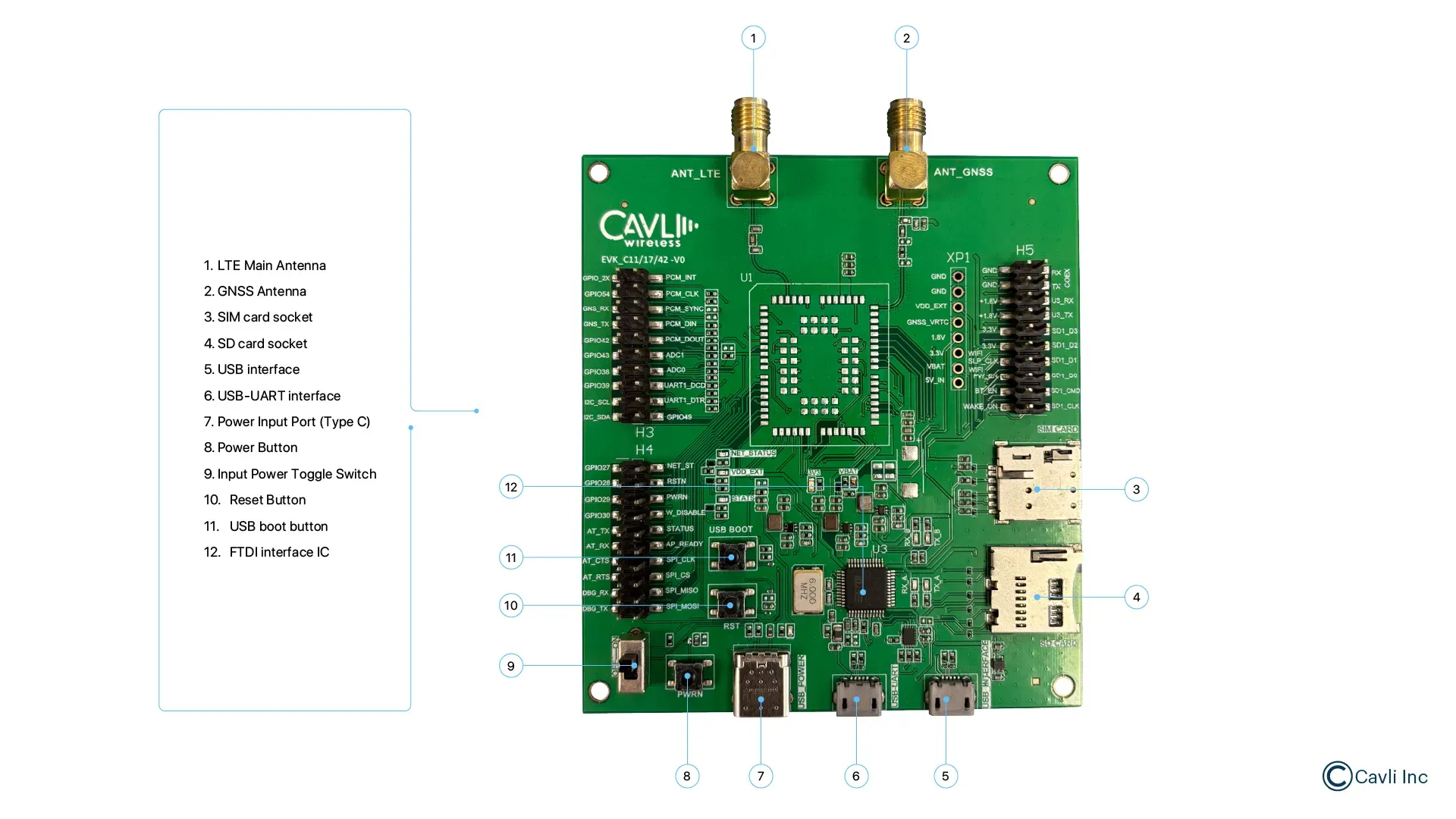
What is an EVK Kit or DevKit?
An Evaluation Kit (EVK) or Development Kit (DevKit) is a pre-assembled hardware kit containing microcontrollers, SoCs, sensors, and connectivity modules designed for prototyping and testing. These kits allow engineers to:
- Evaluate the performance and features of a module or chip.
- Develop firmware and software before final PCB design.
- Test compatibility with other peripherals and interfaces.
- Validate power consumption, signal integrity, and network connectivity.
Why do OEMs and ODMs First Purchase an EVK Kit or DevKit?
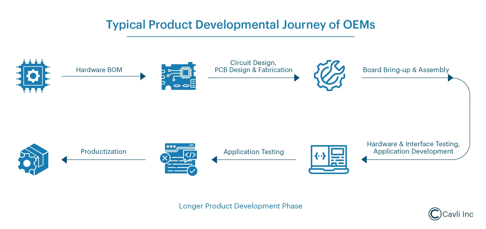
For OEMs and ODMs, the journey from concept to product launch involves multiple stages, such as prototyping, testing, and validation. One of the most crucial first steps is purchasing an EVK (Evaluation Kit) or DevKit (Development Kit). These kits help engineers test functionality, accelerate development, and reduce risks before moving into full-scale production.
Rapid Prototyping & Concept Validation
Before investing in custom PCB design, proof of concept (POC) is essential. EVK kits help OEMs/ODMs validate product feasibility quickly and at a lower cost.
For example, an ODM developing a smart parking sensor can test NB-IoT connectivity using an EVK kit without building a custom board.
Firmware Development & Testing
Firmware development is time-consuming and complex. An EVK allows early firmware testing on actual hardware, enabling debugging and optimization.
For example, with the Cavli C17QS EVK, engineers can develop and test AT commands and MQTT communication before the custom hardware gets ready.
Interface & Compatibility Testing
It ensures compatibility with other peripherals, sensors, or communication interfaces. For example, integrating a GNSS module with an IoT tracker using an LGA cellular module and verifying UART or SPI communication.
Power Consumption Analysis
Battery-operated IoT devices require optimized power consumption. EVKs provide real-time power profiling to maximize battery life. For example, test an NB-IoT module EVK to analyze Power Saving Mode (PSM) and eDRX settings to extend battery life in remote sensors.
Accelerating Time to Market (TTM)
Pre-certified EVKs reduce development time, allowing OEMs to launch products faster. For example, an OEM developing an industrial IoT gateway can quickly prototype and validate connectivity using a Cavli C17QS EVK, reducing TTM.
Reducing Time to Market for OEMs/ODMs with LGA Modules and DDK Kits
LGA modules help IoT pioneers and product designers reduce Time to Market (TTM) with the following:
Faster Prototyping & Scalable Production
- Pre-certified LGA IoT modules (e.g., Cavli C17QS) eliminate the need for extensive RF certification.
- LGA modules are socket-friendly, allowing easy replacement or upgrades in PCB layouts.
- Integration-ready interfaces (UART, SPI, I2C, PCIe) speed up development.
Simplified PCB Design & Assembly
- Surface-mount assembly using automated pick-and-place machines accelerates PCB manufacturing.
- No through-hole soldering is required, unlike PGA-based designs.
- Optimizes BOM, thereby eliminating additional components (e.g., RF shielding and power regulators).
Ready for Mass Production
- LGA modules are designed for high-volume production with better yield rates.
- OEMs and ODMs can rapidly scale production with automated surface mount technology (SMT) assembly.
TOM Reduction With LGA EVK/DDK Kits
In summary, with the LGA module or EVK/ DDK kit, the streamlined process becomes
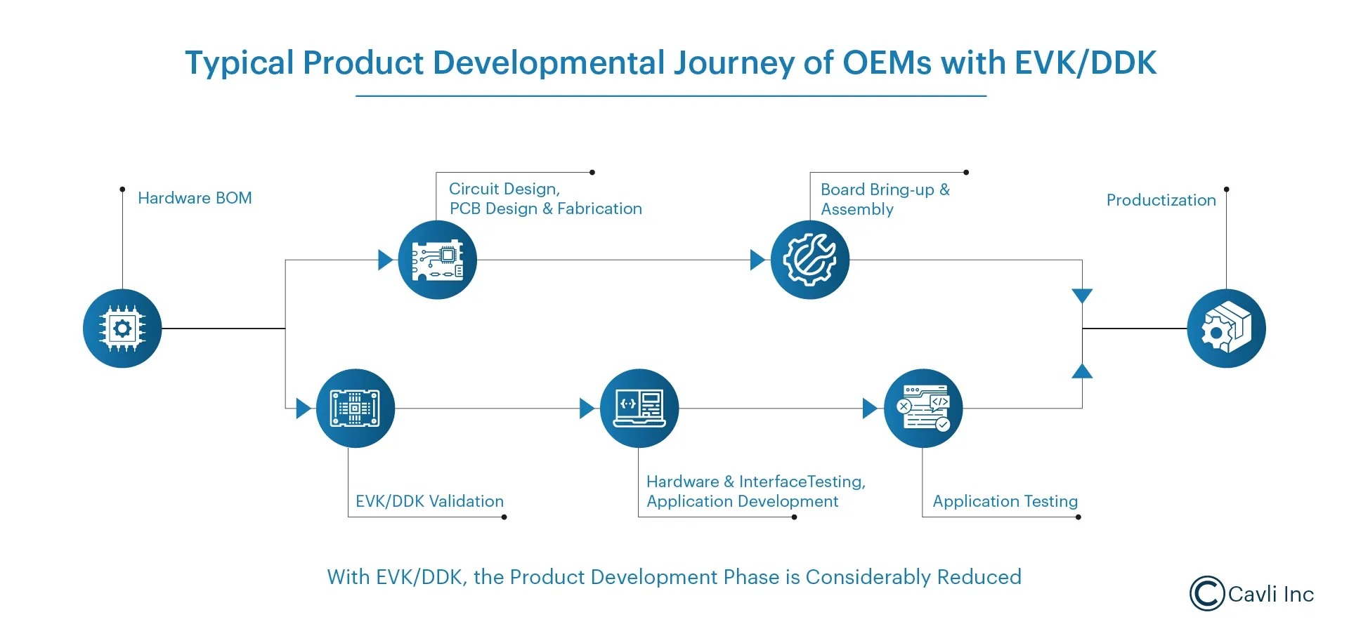
1. Hardware Optimization and Prototyping
- Select the Cavli Cellular IoT Module best suited for your application, choosing the predesigned and developed EVK/DDK kit for that module.
2. Hardware and Interface Testing
- Skip developing circuits and/or PCBs from scratch.
- Test interfaces directly on EVK without complex firmware.
- Engage in custom product development as an additional feature with DDKs.
- Simplify cellular debugging with built-in AT commands.
3. PCB Design and Assembly
- Develop a Simplified Circuit Design with a pre-defined PCB footprint, built-in power regulation, and SIM features based on your respective use case requirements.
4. Firmware and Cloud Setup
- Load the prebuilt Cavli firmware stack to onboard your Cavli module to Cavli Hubble™, our proprietary Cloud-based Connectivity and Modem Management Platform, to test real-time data transmission.
5. Mass Production and Deployment
- With the introduction of DDKs, product development no longer faces delays due to custom PCB design and fabrication. This enables our customers to accelerate their time-to-market, gaining a competitive edge in the IoT industry.
How does the Land Grid Array help optimize BOM for OEMs/ODMs?
Reducing the Bill of Materials is a key factor in lowering manufacturing costs. LGA IoT modules contribute by:
- Eliminating Through-Hole Components: No PGA pins or connectors are required.
- Reducing PCB Layer Complexity: Supports multi-layer boards with high pin density.
- Lowering Assembly Costs: SMT-based designs reduce manual labor.
- Minimize Power Consumption: Efficient current delivery reduces VRM (Voltage Regulator Module) costs.
- Integrating RF Components: Many LGA IoT modules have built-in antennas, reducing external RF module costs.
For example, using an LGA-based LTE/NB-IoT module instead of a discrete modem solution can reduce the component count by 30-40%.
Increasing ROI with LGA-Based IoT Modules in IoT Design
Lower Cost Per Unit
- LGA modules simplify PCB manufacturing, reducing overall assembly and testing costs.
- Less manual labor is required due to SMT-ready designs.
Higher Product Reliability
- No fragile pins = lower failure rates in industrial and automotive applications.
- Reduced RMA (Return Merchandise Authorization) rates increase long-term profitability.
Faster Market Entry = Higher Revenue
- Pre-certified LTE, NB-IoT, and AI modules reduce certification time, allowing quicker product launches.
- IoT integrators can expand into new markets (Industry 4.0, Smart Healthcare, Smart Grids) faster.
Scalability for Future-Proof IoT
- LGA modules support 5G, AI, and future LPWAN standards, allowing long-term product roadmaps.
- Easier field upgradability via OTA (Over-the-Air) firmware updates.
Closing Notes
With cellular IoT, the demand for compact, scalable, and high-performance solutions has never been greater. The LGA (Land Grid Array) form factor offers unmatched benefits that OEMs and ODMs cannot afford to overlook.
With its rugged, pinless design, LGA eliminates the mechanical fragility of traditional packages, providing enhanced durability for your IoT devices, even in harsh environments. LGA modules with automated SMT processes reduce production costs, minimize human error, and significantly shorten time to market, allowing you to scale production efficiently and remain competitive. With high-volume, automated production and better thermal performance, LGA-based IoT modules accelerate your development cycles.
As we transition to 5G, LGA modules are future-proof, providing flexible support for multi-band connectivity and high-speed data transfer, ensuring that your devices remain compatible with evolving network standards.
Now, more than ever, the LGA form factor is not just an option—it is a strategic necessity for all looking to remain competitive in the fast-paced IoT market. Whether you are designing smart meters, connected vehicles, industrial sensors, or healthcare devices, LGA-based cellular modules offer a clear edge in reliability, scalability, and manufacturing efficiency.
Go Beyond and Explore
What is a Flip-Chip Land Grid Array?
Key Features of Flip-Chip Land Grid Array
Flip-Chip Technology: Flip-chip refers to a packaging method where the chip is flipped upside down so that its active surface (the side with the contacts or bumps) faces the PCB. In the Flip-Chip Land Grid Array, the flip-chip die is directly connected to the PCB using solder bumps instead of the traditional wire bonding process. It allows for shorter interconnects, faster data transfer, and better signal integrity. Land Grid Array (LGA) Design: LGA is a packaging design where the chip's contact pads (lands) are arranged in a grid pattern on the bottom of the chip rather than using pins or solder balls. In the Flip Chip Land Grid Array, the chip's active surface with solder bumps is aligned with the LGA contact pads on the PCB. The pads on the PCB enable the electrical connection between the chip and the board.Advantages of Flip Chip Land Grid Array
- Higher Density: The flip-chip method allows for a higher-density connection between the chip and the PCB, which results in a smaller package size and the ability to fit more pins (lands) in a compact area.
- Improved Electrical Performance: Flip-chip bonding reduces electrical resistance and inductance, improving the signal integrity and data speed of the device.
- Better Thermal Management: The flip-chip design can enhance thermal dissipation, as the chip's heat-generating area is in direct contact with the PCB, which improves overall thermal performance.
- Higher Reliability: With no exposed pins, as seen in traditional PGA or BGA, FC-LGA is more mechanically robust and less prone to damage during handling or over the device's lifespan
What are the most favorable applications for LGA-based modules?
- LGA packages offer a compact size for space-constrained devices like wearables, smart meters, and asset trackers.
- It offers high performance for IoT applications like industrial automation, healthcare IoT devices, and smart cities.
- Thermal and mechanical reliability in rugged environments makes it ideal for remote sensors, smart agriculture, and automotive IoT.
- It is scalable across multi-band IoT solutions, from NB-IoT to 5G-enabled devices.
What are typical LGA pad counts and how do they affect the module's capabilities?
- LGA 1151 (used for desktop CPUs) typically has 1,151 pads.
- LGA 2011 (common in server processors) has around 2,011 pads.
- For cellular IoT modules, LGA pad counts typically range from 100 to 500 pads, depending on the connectivity and features required (e.g., LTE, NB-IoT, or 5G).
Author

Drishya Manohar
Sr. Associate - Content Marketing